India’s first Advanced Packaging Substrate Project in Odisha
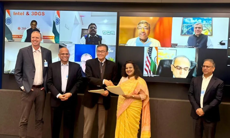
Odisha: The Odisha government has signed a landmark Memorandum of Understanding (MoU) with US-based technology companies Intel and 3D Glass Solutions (3DGS) to establish a state-of-the-art advanced packaging substrate manufacturing facility in the state. According to government officials, the project will be the first of its kind in India, marking a major milestone in the electronics manufacturing sector.
An official statement issued on Friday stated that the proposed facility will be based on advanced glass-based substrate technology and high-density interconnect packaging, technologies crucial for the manufacture of modern electronic chips and high-performance systems.
According to the government, the project will play a vital role in meeting the needs of rapidly growing sectors such as artificial intelligence (AI), high-performance computing, telecommunications, and next-generation electronics. The facility is expected to strengthen advanced semiconductor and electronic packaging technology in India.
Under the agreement, Intel will serve as the technology partner for the project. The company will collaborate on process expertise, technology licensing, quality systems, and workforce capacity building. Intel will also provide technical guidance and necessary training support for the project.
Government officials stated that 3D Glass Solutions (3DGS) will also play a key role in the project, particularly in the areas of advanced glass substrate technology and design innovation. This partnership is considered a major step towards bringing global-level technology to India.
The opening of this facility will strengthen Odisha’s plan to develop into a high-tech manufacturing hub. It is also expected to create new job opportunities and promote technical skill development in the state.
The government believes that this project will be a milestone for the electronics ecosystem not only in Odisha but across the country. It will help India gain a strong foothold in the global semiconductor and advanced packaging supply chain.
According to officials, a detailed plan will be prepared for the implementation of this project in the coming time and it will be taken forward in a phased manner by coordinating with the concerned agencies.